
FPGA (Field Programmable Gate Array) is a field programmable gate array. It is a product of further development based on programmable devices such as PLA, PAL, GAL, and CPLD. It is a semi-custom circuit in the field of application-specific integrated circuits (ASIC), which not only solves the shortcomings of custom circuits but also overcomes the shortcomings of the limited number of original programmable device gates.
1. FPGA Introduction
FPGAs are commonly used to implement digital circuit modules. Users can reconfigure logic modules and I/O modules inside the FPGA to meet user needs. It also features static re-programmability and dynamic system refactoring, allowing hardware functions to be modified programmatically like software. It is no exaggeration to say that an FPGA can perform any digital device function, down to a simple 74 circuit, up to a high-performance CPU, can be implemented with an FPGA. FPGAs are like a piece of white paper or a stack of wood, and engineers can freely design a digital system using traditional schematic input methods or hardware description languages.
2. The History of FPGA Development
The development history of FPGA is shown in the figure below. Compared with PROM, PAL/GAL, and CPLD, FPGAs have higher scale performance.
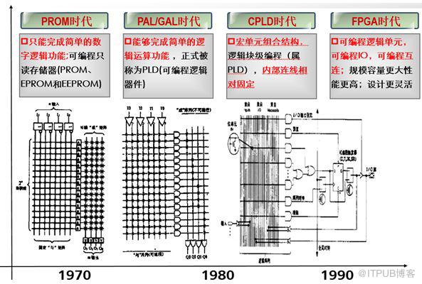
Figure 1 History of FPGA development
The mainstream manufacturers of FPGA chips include Xilinx, Altera, Lattice, and Microsemi, with the first two market shares totaling 88%. At present, all mainstream FPGA manufacturers are American manufacturers. Domestic FPGAs started at least 20 years later than the United States, and are still in the growth stage, limited to the low end, and have not matured in the communication market.
In December 2015, Intel acquired Altera Corporation for $16.7 billion. Shortly after the acquisition, Altera developed a product roadmap for integrating Intel processors with FPGAs. The benefit of these two product integrations is the ability to deliver innovative heterogeneous multi-core architectures that meet the needs of new markets such as artificial intelligence while dramatically reducing power consumption.
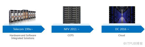
Figure 2 FPGA application history in the field of telecommunications
FPGAs are very mature and widely used in aerospace, military, and telecommunications. Taking the telecommunications field as an example, in the telecom equipment integration stage, the FPGA is analyzed by the application network protocol and interface conversion due to its programming flexibility and high performance.
- In the NFV (NetworkFunction Virtualization phase, the FPGA implements 5 times performance improvement of the network data surface based on the general server and the hypervisor, and can be managed by the general OpenStack framework.
- In the cloud era, FPGA has been used as a basic IaaS resource to provide development services and acceleration services in the public cloud. AWS, Huawei, and BAT all provide similar services.
- To date, Intel’s Stratix 10 devices have been successfully applied to the Brainwave project of the Microsoft Real-Time Artificial Intelligence Cloud Platform.
3. Recent Developments of Two Mainstream FPGA Companies
Xilinx has focused on chip leadership and a rich acceleration solution, gaining support for mainstream cloud platforms through open strategy and establishing its leading position in the data center. Its UltraScale+ series of FPGAs has been a leader for more than a year, making it a leader in cloud platform competition. Its VU9P devices are widely used in cloud computing platforms of companies including AWS, Baidu, Ali, Tencent, and Huawei.
To meet the increasing performance demands of FPGA chips in the accelerator field, Xilinx has released the next-generation ACAP chip architecture for data centers and the introduction of 7nm Everest devices. This device is no longer a traditional FPGA. It integrates ARM, DSP, Math Engine processor array and other cores and will be mass-produced in 2019. Compared to the VU9P, Everest supports AI processing performance that can be increased by a factor of 20.
Intel offers a full-stack solution from hardware to the platform to application. It does not open up hardware and platform design to avoid ecological fragmentation, and the investment is huge but slow.
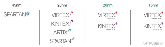
Figure 3 Xilinx product line diagram
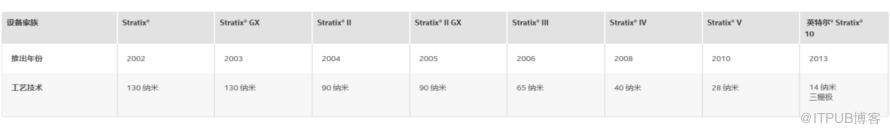
Figure 4 Intel (with the Stratix series as an example) product technology era
There are certain technical difficulties in the practical application of FPGA in the data center server market, including the following aspects:
- 1. Higher programming threshold: The hardware description language is different from the software development language, which requires developers to have a deeper understanding of the underlying hardware; therefore, talent has become an important factor limiting FPGA applications. It is understood that the current personnel engaged in FPGA development in China is estimated to be about 20,000 people.
- 2. Integration is difficult: FPGA development and application require software and hardware coordination, including system modeling using a high-level language, hardware code (circuit) design, hardware code simulation, joint debugging of underlying driver software and hardware logic, and so on.
- 3. The development cycle is relatively long compared to software: hardware development is more complicated than software development, and the debugging cycle is also lengthened.
- 4. It is difficult to obtain an independent logical IP.
4, The Overall Structure of the FPGA
The FPGA architecture mainly includes four parts: a Configurable Logic Block (CLB), an Input-Output Block (IOB), an Interconnect, and other embedded units.
CLB is the basic logic unit of an FPGA. The actual number and characteristics will vary from device to device, but each CLB contains a configurable switch matrix consisting of 4 or 6 inputs, several selection circuits (multiplexers, etc.) and flip-flops. The switch matrix is highly flexible and is configured to handle combinatorial logic, shift registers or RAM.
FPGAs support a wide range of I/O standards, providing an ideal interface bridge for system design. The I/O in the FPGA is grouped by the bank, and each bank can independently support different I/O standards. Today’s state-of-the-art FPGAs offer more than a dozen I/O banks that provide flexible I/O support.
The CLB provides logic performance, and flexible interconnect routing is responsible for passing signals between the CLB and the I/O. There are several types of routing, from global low-skew routing designed to implement CLB interconnects (short-line resources) to high-speed horizontal and vertical long lines (long-line resources) within the device, to clocks and other global signals (global-specific Wiring resources). In general, the design software of each manufacturer hides the interconnect routing tasks, which are invisible to the user, thus greatly reducing the design complexity.
The embedded hardcore unit includes RAM, DSP, DCM (Digital Clock Management Module) and other specific interface hard cores. The internal structure of the FPGA device is as follows.
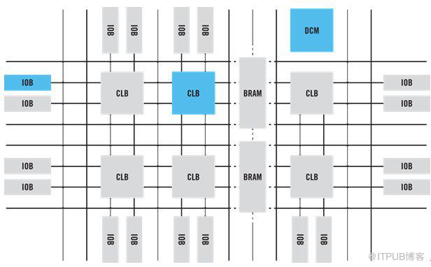
Figure 5 internal structure of the FPGA device
In general, the larger the device model number, the larger the logical resources that the device can provide. In the FPGA device selection, users need to compare this table according to the business logic resources (CLB), internal blockRAM, interface (high-speed Serdes logarithm), digital signal processing (DSP hardcore) and future expansion. Consider the most appropriate logic device for the project.
5. FPGA Development Process
The FPGA design flow is the process of developing FPGA chips using EDA development software and programming tools. The development process of FPGA is generally as shown in the following figure, including the main steps of function definition/device selection, design input, function simulation, logic synthesis, place and route, and implementation, and programming debugging.
1. Function definition/device selection: Before the start of the FPGA design project, there must be a definition of system functions and division of modules. In addition, according to task requirements, such as the function and complexity of the system, the working speed, and resources of the device itself. Trade-offs, costs, and the availability of connections choose the right design and the right device type.
2. Design input: Design input refers to the use of hardware description language to express the designed system or circuit with code. The most common hardware description language is Verilog HDL.
3. Functional simulation: Functional simulation refers to the verification of the logic function of the circuit designed by the user before the logic synthesis. Before the simulation, it is necessary to set up the test platform and prepare the test stimulus. The simulation result will generate the report file and the output signal waveform, from which the signal changes of each node can be observed. If an error is found, return to the design modification logic design. Common simulation tools include Model Tech’s ModelSim and Sysnopsys’ VCS software.
4. Logic synthesis: The so-called synthesis is to transform the description of the higher level abstraction level into a lower level description. The integrated optimization optimizes the generated logical connections according to the target and requirements and planarizes the hierarchical design for FPGA layout software. At the current level, comprehensive optimization refers to compiling design inputs into logically connected netlists composed of basic logic units such as AND gates, OR gates, NOT gates, RAMs, and flip-flops, rather than real gate-level circuits.
Real and specific gate-level circuits need to be generated by the FPGA manufacturer’s place-and-route function based on the synthesized standard gate-level structure netlist. In order to be converted into a standard gate-level netlist, the HDL program must be written to match the style required by a particular synthesizer. Commonly used synthesis tools include Synplicity’s Synplify/Synplify Pro software and comprehensive development tools from various FPGA vendors.
5, layout and implementation: layout can be understood as the use of tools to map the logic to the resources of the target device structure, determine the optimal layout of the logic, select the logic and the input and output function link routing channel to connect, and generate corresponding Files (such as configuration files and related reports); implementation is to configure the integrated generated logical netlist to a specific FPGA chip. Since only the FPGA chip manufacturer knows the chip structure best, the layout and wiring must choose the tools provided by the chip developer.
6, programming and debugging: the final step of the design is programming and debugging. Chip programming refers to the generation of the user data file (bitstream data file, Bitstream Generation), loading the programming data into the FPGA chip; then the upper board test can be performed. Finally, the FPGA file (such as a .bit file) is downloaded from the computer to the FPGA chip on the board.
6. How to Use FPGA
After the FPGA is developed, the verified load file is finally obtained. After outputting the load file, normal business processing and verification can be started (using the software loading method as an example to describe the whole process)
- 1, logical loading;
- 2. After the board software loads the logic, it needs to reset the logic.
- 3. After the reset is completed, the software needs to wait for a period of time until the logic phase-locked loop works stably;
- 4. The software starts the self-check operation of the logic external RAM, internal block RAM, DDRC, etc.
- 5. After the software completes the self-test, it initializes all the writable RAM space and registers of the logic;
- 6, initialization is completed, the software refers to the logic chip manual configuration table entries and registers;
- 7. The logic is ready to start processing the business.
7. FPGA Application Scenarios
FPGA is suitable for non-regular multi-concurrency, intensive computing and protocol parsing scenarios, such as artificial intelligence, gene sequencing, video coding, data compression, image processing, network processing and other areas of acceleration.
Original Article Source from http://www.itpub.net/2019/05/23/1931/