The expansion of the optical transceiver market is driven by the demand for cloud computing, the Internet of Things, and Ethernet acceleration in virtual data centers. The current speeds of 10 gigabits per second (bps), 40 Gbps and 100 Gbps will soon be overwhelmed by 200 Gbps and 400 Gbps. As the speed increases, the power consumption of the optical transceiver module also increases, but the shape must remain the same. As a result, module designers are under intense pressure to use highly integrated chips with the lowest possible power consumption. How can you achieve more functionality while supplying power more efficiently in a tight space? This article introduces a power management system that efficiently supplies power in a small space and enables higher speeds than expected with next-generation optical transceivers.
Optical network interface
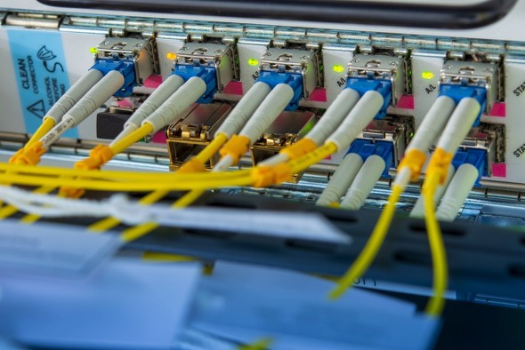
In optical network interfaces, communication devices such as switches ( Figure 1 ) and routers are located far away (up to several kilometers) from each other and connected with fiber optic cables. The switch or router processes the information packet, and the transceiver interfaces with the cable and converts the received optical signal into electrical impulses (and vice versa).
Optical transceiver
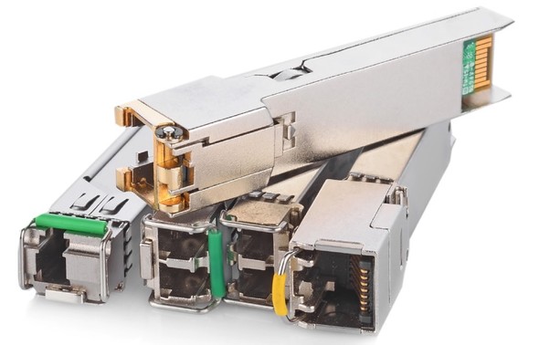
Fiber optic transceivers ( Figure 2 ) are an important component of fiber optic transmission networks. These transceivers are designed in a compact form and incorporate an optical subassembly that is ideal for high-density networks.
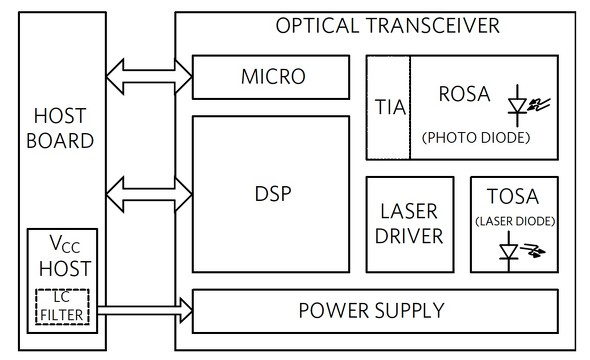
The main components of the transceiver module ( Figure 3 ) are the transmitter light subassembly (TOSA) and the receiver light subassembly (ROSA). The TOSA consists of a laser diode, an optical interface, a monitor photodiode, a metal / plastic enclosure, and an electrical interface. ROSA consists of a photodiode, an optical interface, a metal / plastic enclosure, and an electrical interface. A transimpedance amplifier (TIA) converts the photodiode current into a differential voltage for further processing. The DSP (Digital Signal Processor) / PHY (Physical Layer) on the board coordinates the communication protocol, and the microcontroller configures the DSP / PHY, optical subassembly and regulator. Each component of the module is powered by a power supply on the board that receives the VCC input (3.3 V) from the host board. This 3.3V is supplied through a powerful filter to smooth the peak of current consumed by each component of the transceiver.
State-of-the-art double line density (QSFP-DD) optical transceivers with quadruple bandwidth, small geometry, and pluggable capabilities have eight output classes. Higher classes support higher data rates and longer cable distances. For example, Class 1 has a peak power of 1.5W and a peak current of 600mA, usually corresponding to speeds of 40Gbps and maximum link lengths of 300m. Class 7 is expected to provide up to 2 km transmission distance at 400 Gbps with 14 W peak power and 5.6 A peak current. Class 8 is the highest power output (14 W or more, 6 A steady state current).
Transceiver power supply
The transceiver module power tree shown in Figure 4 represents the typical current and voltage range of DSP / PHY digital, analog, PLL (phase locked loop) rails powered by multiple output voltage regulators (TRIPLE BUCK). The optical interface (laser driver, TIA, ROSA, TOSA) is powered by a single regulator (BUCK). The input of the microcontroller (MICRO) receives 3.3 V directly. The buck converter needs to be very efficient to ensure that the input power is kept within the device class power envelope.
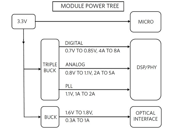 Figure 4: Transceiver Power Tree
Multiphase architecture
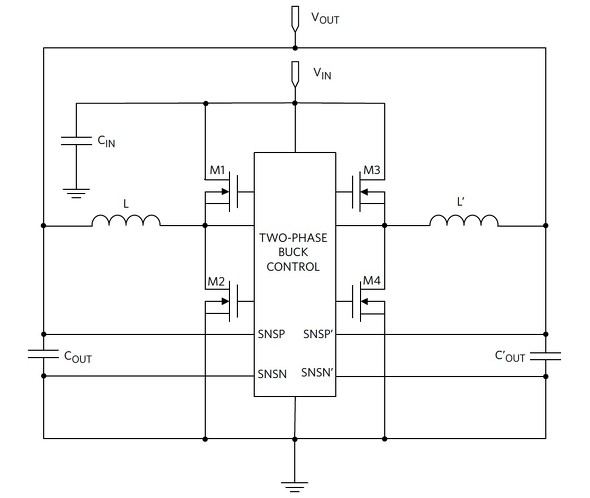
For digital rails that require up to 8A peak current, a two-phase interleaved synchronous buck converter architecture, as shown in Figure 5, is the best solution.
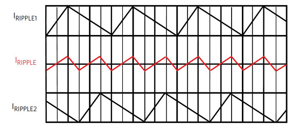
The two interleaved phases guarantee reduced ripple current and hence reduced ripple voltage. Low total ripple current is achieved at relatively low operating frequency per phase. As an example, Figure 6 shows that for two ripple currents with 180% antiphase and 33% duty cycle, the total ripple current is half as large as a single phase at twice the frequency. The lower output current ripple and higher voltage ripple available at the higher frequency means that fewer capacitors are required at the output, which leads to reduced BOM.
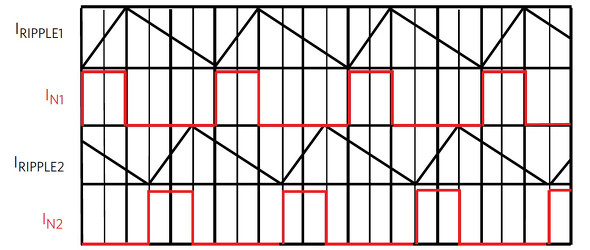
The two-phase architecture also reduces the number of input capacitors required. The total input current is the sum of two antiphase currents ( I IN1 and I IN2 in Figure 7 ). Here, by distributing the total input current in the time direction, the total RMS value of the input current is reduced compared to single-phase operation, and a smaller input current ripple filter can be used.
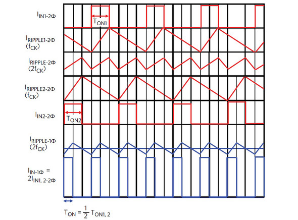
Furthermore, as shown in Figure 8, two phases (shown in 22, red) are more efficient than single phases (shown in 1Φ, blue) when the two schemes are operated at the same output ripple frequency. Even single-phase operation can achieve high frequency and low current ripple by operating at twice the switching frequency (fSW) of two phases, but the switching loss will be larger. Although the number of transitions of the two schemes in one cycle is the same, the current consumption of the two-phase converter is half the current (at twice the time) of the single-phase converter, thus reducing switching loss.
Another great advantage of 2-phase converters is a fast transient response and reduced voltage overshoot / undershoot during load steps. Half current per phase, low current ripple and double ripple frequency allow the switching frequency to be increased further reducing component size and converter closed-loop bandwidth without reaching temperature limits Can be increased.
Finally, as the total load current increases, the size of the passive components also increases. At high loads, single-phase buck inductors are large and inefficient. Multiphase operation reduces the current in the individual phases, ensuring the optimal size of the passive components.
Single-phase to 4-phase, 1 to 4 outputs, maximum 20A, the configurable buck converter
As an example, a configurable single phase to four phases, one to four output high current, buck (step-down) converter is shown in FIG. shows. The device’s high efficiency, small footprint, high output voltage accuracy, fast transient response, and fast serial interface options make it suitable for powering DSP / PHY applications in optical transceiver applications. Flexible architecture: “4” (one four-phase output), “3 + 1” (two outputs, one three-phase and one single phase), “2 + 2” (two two-phase outputs), “2 + 1” (three A phase configuration such as output, one two-phase, two single-phase), “1 + 1 + 1 + 1” (four single-phase outputs) is possible.
System power handling with the single chip
By choosing the appropriate configuration, one IC can power the DSP / PHY of the optical transceiver in Figure 3. In Figure 9, the DSP / PHY digital, analog, and PLL sections can be powered in a “2 + 1 + 1” configuration.

Efficiency
The two-phase efficiency curve of this device is shown in Figure 10 with currents up to 10 A (0.22 μH, 2520 size inductor).

The two-phase architecture provides high efficiency even at very low duty cycles (low VOUT).
The single-phase efficiency curve of this device is shown in Figure 11 (0.22μH, 2520 size inductor) for currents up to 5A.

High efficiency, ultra-compact single buck converter
The single-phase buck converter in Figure 4 can be implemented with the application circuit shown in Figure 12 .

Figure 13 shows the efficiency curve at the 1.8V output. This solution provides excellent efficiency of + 90% over most of the operating range.

The space occupied by this application circuit is approximately 7 mm 2 .
Summary
We discussed the challenges of optical transceivers to provide high data rates within the constraints of maximum power consumption allowed by each class of QSFP-DD devices. The single-phase to four-phase, one- to four-output, high-current buck regulators are suitable for powering high data rate optical transceivers due to their high efficiency and small PCB size.
Original Article Source from https://ednjapan.com/edn/articles/1902/15/news009_3.html